broadcom and nvidia to harness tsmc's silicon photonics
Hsinchu, Monday, 30 December 2024.
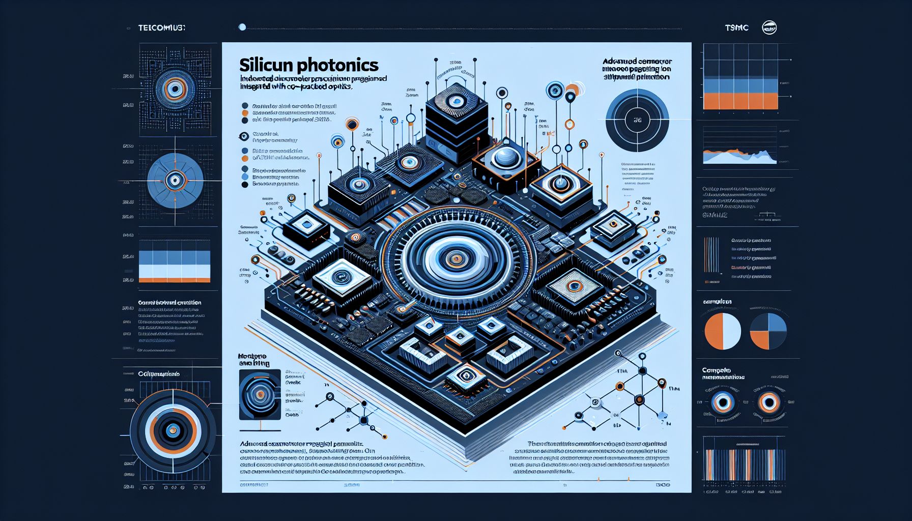
Taiwan Semiconductor Manufacturing Company (TSMC) is making strides in silicon photonics, integrating Co-Packaged Optics (CPO) with advanced semiconductor packaging. Broadcom and NVIDIA are set to be the first to pilot this technology, marking a significant advancement in the semiconductor industry. TSMC’s innovation aims to overcome the speed limitations of traditional copper interconnects, facilitating 1.6T optical transmission. The development is expected to enter the sample shipment phase in early 2025, with full-scale deployment anticipated by late 2025. This collaboration with Broadcom includes successful trials of Micro-Ring Modulators using a 3nm process. As the industry gears up for the silicon photonics era, TSMC’s advancements could revolutionize computing and data transmission speeds. However, due to complex packaging processes, some orders may be outsourced, highlighting the challenges in achieving high yield rates.
Market leadership through technical breakthroughs
TSMC’s recent completion of CPO integration with advanced semiconductor packaging technology represents a significant technical achievement [1]. The successful trial production of Micro-Ring Modulators (MRM) on 3nm process with Broadcom [1] strengthens TSMC’s position in next-generation semiconductor technology. This development aims to eliminate traditional copper interconnect limitations [2], potentially revolutionizing data transmission capabilities in high-performance computing applications.
Production timeline and capacity expansion
The company plans to begin sample shipments in early 2025, with mass production of 1.6T optical transmission products scheduled for the second half of 2025 [1]. Full-scale shipments are projected for 2026 [1]. TSMC’s manufacturing capabilities have shown remarkable growth, with over 150 customer product tape-outs completed by the end of 2024 [3]. The company’s CoWoS technology is targeting advanced configurations featuring SoIC and 12 HBMs by 2027 [3].
Strategic implications for AI computing
NVIDIA’s involvement is particularly strategic as the company seeks to overcome current limitations in its GPU interconnect technology [1]. The current NVLink system only allows for 72 GB200 chips to interconnect, but CPO technology integration in future GPU generations, including the GB300 and Rubin architecture, could significantly expand these capabilities [1]. This advancement addresses critical issues of signal interference and overheating in high-performance computing systems [1].
Manufacturing challenges and industry collaboration
Despite the technological advances, TSMC faces challenges in CPO module packaging, including complex procedures and lower yield rates [1]. The company is addressing these challenges through its 3DFabric Alliance [3], established to foster cross-industry collaborations. The introduction of the 3DBlox language in 2024 [3] demonstrates TSMC’s commitment to improving interoperability across chip design and PCB manufacturing processes.