tsmc unveils a14 chip: a leap in ai and efficiency
Santa Clara, Thursday, 24 April 2025.
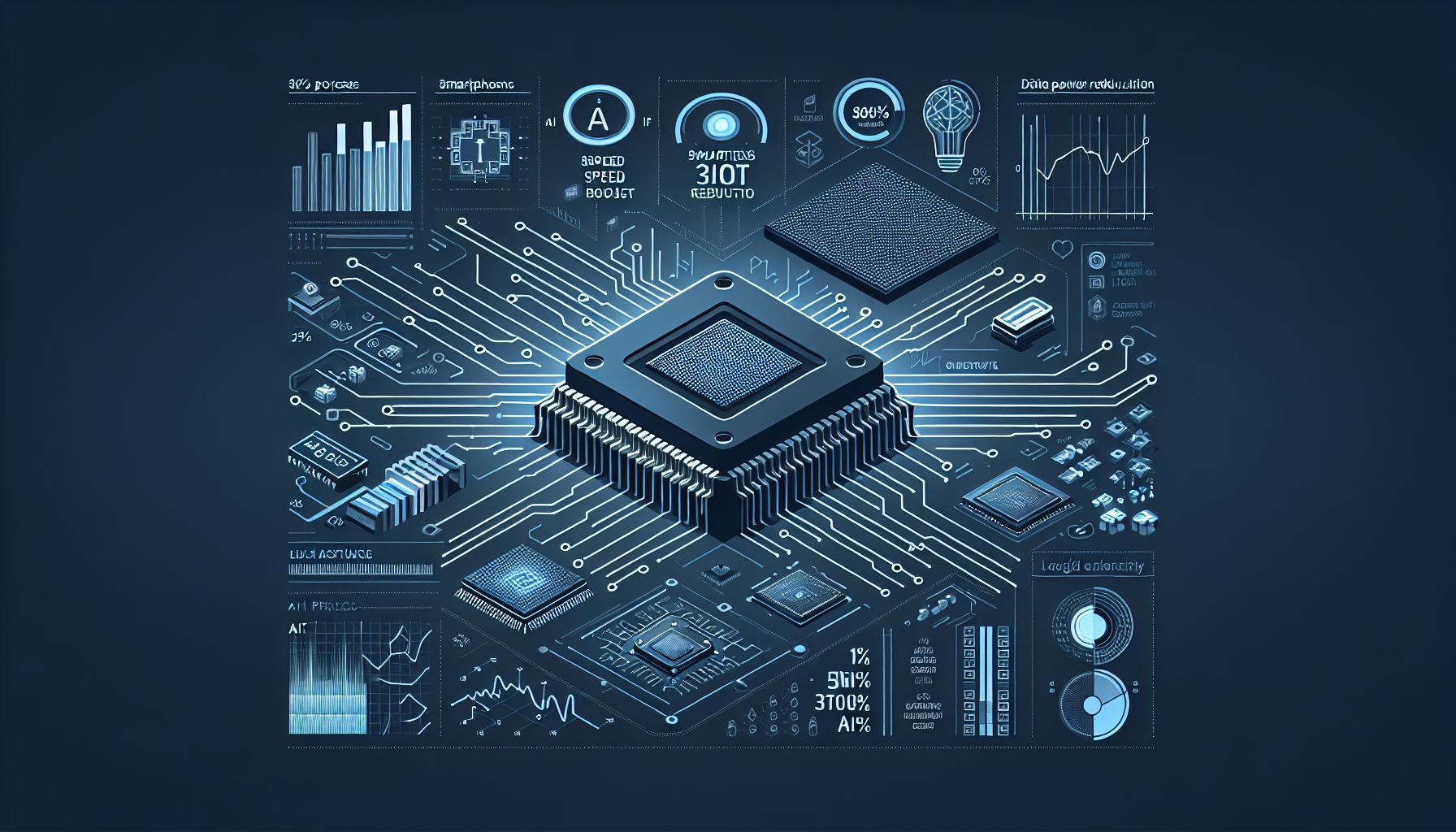
tsmc just announced its A14 process, targeting ai, smartphones, automotive, and iot applications. the a14 process is expected to go into production in 2028. early data suggests up to 15% speed boost or 30% power reduction compared to its n2 process. logic density should increase by more than 20%. the company also evolves its nanoflex architecture to nanoflex pro. the new tech should allow for smarter on-board ai capabilities on smartphones.
A14 and tsmc’s technology roadmap
TSMC’s chairman and CEO, Dr. C.C. Wei, emphasized that the A14 process, along with TSMC’s manufacturing excellence, provides a reliable roadmap for customer innovation [1]. TSMC also introduced new technologies for high-performance computing, smartphones, automotive, and IoT applications [1]. These technologies include advancements in Chip on Wafer on Substrate (CoWoS®) technology and System-on-Wafer (TSMC-SoW™) technology, aimed at enhancing AI capabilities and computing power [1]. TSMC plans to bring 9.5 reticle size CoWoS to volume production in 2027, which will allow for the integration of 12 HBM stacks or more [1].
impact on tsmc stock
TSMC’s stock closed at $157.810 on April 23, 2024, marking a 4.23% increase [2]. The options trading volume for TSMC on the same day was 123,800 contracts, with call options representing 56.9% of the volume and put options accounting for 43.1% [2]. Total open interest for TSMC options was approximately 2,021,200 contracts [2]. TSMC’s unveiling of the A14 process and its related technologies could positively influence investor sentiment, potentially driving the stock price higher as the company positions itself for future growth in key technology sectors [GPT].
manufacturing capacity and geopolitical considerations
TSMC’s continuous innovation in manufacturing processes is crucial for maintaining its market leadership [3]. As the largest dedicated semiconductor foundry in the world, TSMC’s advancements in process technology, like the A14, enable its clients, including Nvidia, Qualcomm, and Broadcom, to develop cutting-edge products [3]. Geopolitical factors also play a significant role, given TSMC’s location in Taiwan [GPT]. Any instability in the region could impact TSMC’s manufacturing capacity and, consequently, the global supply of advanced semiconductors [alert! ‘geopolitical risks are dynamic and difficult to predict precisely’]. TSMC is known to have a strong culture of protecting its trade secrets [3].
collaborations and future technologies
TSMC is collaborating with Cadence and Synopsys on design solutions for AI and 3D-IC chip designs, targeting TSMC’s A16 and N2P process technologies [2]. Synopsys and TSMC are also providing EDA software and IP solutions for digital and analog design flows on TSMC A16 and N2P, building upon their existing collaboration on the A14 process [2]. These collaborations highlight TSMC’s commitment to advancing chip design and manufacturing capabilities [GPT]. TSMC is increasing their investment in advanced packaging technologies [7]. An analyst at TechInsights noted that advancements in chip packaging are crucial for the future of AI [7].
Bronnen
- pr.tsmc.com
- www.futunn.com
- www.tangibly.com
- www.futunn.com
- www.jin10.com
- www.worldjournal.com
- www.cnbeta.com.tw