tsmc kicks off semiconductor production at new Japanese plant
Tokyo, Monday, 30 December 2024.
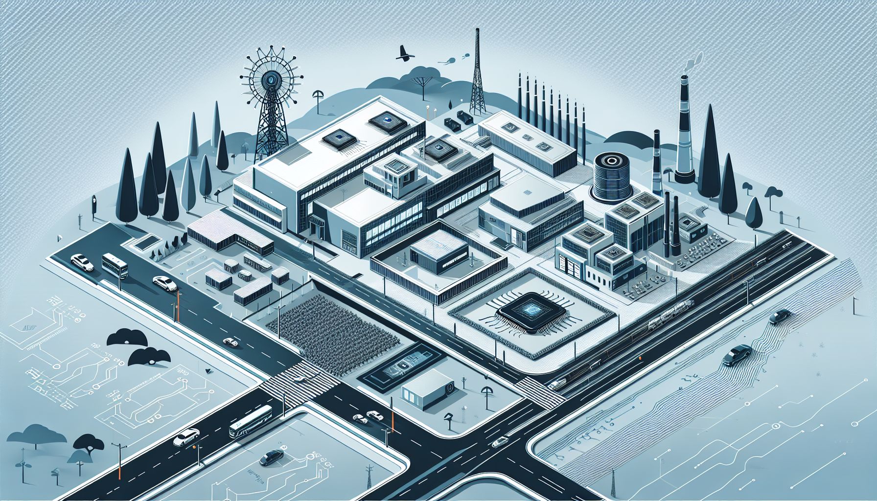
TSMC has started mass production at its new semiconductor facility in Kumamoto, Japan, marking a pivotal move in its global expansion strategy. The plant focuses on producing 12 to 28-nanometer semiconductors, primarily targeting the automotive and image sensor markets. This development represents TSMC’s first major manufacturing site in Japan, underscoring its efforts to strengthen its presence in the global semiconductor supply chain. The new facility is a collaborative project with Sony and Denso, with significant financial backing from the Japanese government. TSMC plans to add a second plant by 2027, which will produce more advanced 6 to 7-nanometer chips. This expansion is expected to reinforce Japan’s position in the global semiconductor industry while supporting TSMC’s strategy to diversify its manufacturing locations amid geopolitical tensions. The project highlights Japan’s ambitions to boost its semiconductor sector and reduce reliance on foreign technology.
Investment and collaboration details
The Kumamoto facility represents a significant investment of $8.6 billion [4], with substantial support from the Japanese government providing $7.8 billion in subsidies [4]. The project brings together industry giants TSMC, Sony, and Denso in a strategic partnership [3][4]. The facility’s initial monthly production capacity is set at 55,000 wafers [4], focusing on manufacturing logic semiconductors for image sensors and automotive applications [3].
Technology capabilities and expansion plans
The first plant specializes in 12 to 28-nanometer process technologies [1][3], while a second facility, scheduled to begin construction next year, will produce more advanced 6 to 7-nanometer chips [1]. The combined investment for both facilities is projected to reach $22.5 billion [3], with the second plant expected to commence operations by the end of 2027 [1][4]. Once both facilities are operational, their combined monthly production capacity will exceed 100,000 wafers [4].
Strategic importance for Japan
As the world’s third-largest semiconductor consumer [4], Japan views this facility as crucial for strengthening its domestic semiconductor supply chain [5]. The plant creates approximately 1,700 jobs in the region [5] and represents a significant step in Japan’s efforts to reduce dependence on foreign technology [5]. The facility’s launch on December 28, 2024 [5], marks a milestone in Japan’s semiconductor industry revival [1].