Swedish startup promises 40% cost cut in advanced chip manufacturing
Tokyo, Thursday, 28 November 2024.
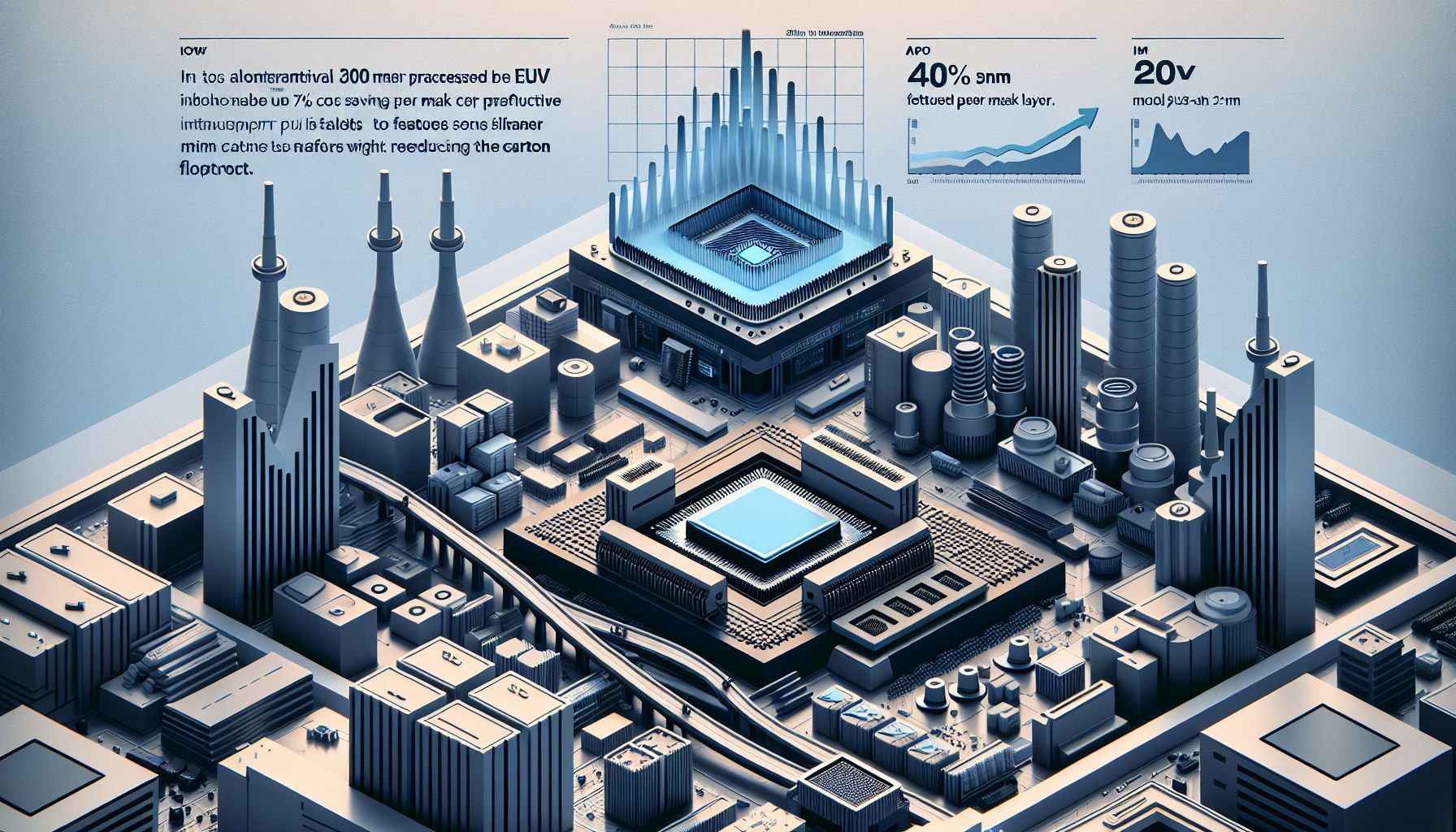
AlixLabs is set to transform semiconductor manufacturing with its groundbreaking 300mm wafer processing equipment debut at SEMICON Japan. The Swedish company’s APS technology offers a game-changing alternative to expensive EUV lithography, promising up to 40% cost savings per mask layer in sub-7nm chip production. This innovation enables manufacturers to create features smaller than 20nm while reducing carbon footprint. As Japan aims to revitalize its semiconductor industry, AlixLabs’ technology could be pivotal in making advanced chip production more accessible and sustainable. The system has already demonstrated impressive capabilities, achieving 15nm precision on silicon and 3nm on gallium phosphide, positioning AlixLabs as a potential disruptor in the competitive semiconductor equipment market.
market impact and investor interest
The introduction of AlixLabs’ 300mm wafer processing equipment is generating significant interest from investors. The potential for a 40% reduction in production costs could lead to increased profitability for semiconductor manufacturers. This cost efficiency, combined with the sustainability aspect, aligns with current market trends favoring green technologies. Investors are closely monitoring how this technology could affect AlixLabs’ market share and influence stock performance in the semiconductor sector[1][2].
strategic positioning in japan
AlixLabs is strategically targeting Japan, a country eager to regain its status as a leader in semiconductor production. The company’s presence at SEMICON Japan is a vital step in capturing the attention of major Japanese manufacturers. With the semiconductor industry being a key focus for Japan’s economic revitalization efforts, AlixLabs’ technology could become integral to the nation’s strategy. This could lead to potential partnerships and collaborations, thereby strengthening AlixLabs’ position in the market and potentially boosting its stock value[1][2].
expert opinions on technological advancement
Experts in the semiconductor field have praised the APS technology for its innovative approach to reducing costs and carbon emissions. By offering a viable alternative to EUV lithography, AlixLabs is addressing critical challenges in advanced chip manufacturing. Industry analysts suggest that if AlixLabs can successfully scale its operations and prove the efficacy of its technology in mass production, it could significantly impact the semiconductor industry landscape. This could lead to a reevaluation of current manufacturing processes and prompt a shift towards more sustainable practices[1][2].
future prospects and growth potential
The future looks promising for AlixLabs as it continues to innovate in the semiconductor equipment market. The company’s focus on reducing costs and environmental impact aligns with global trends towards sustainability. As AlixLabs expands its client base and demonstrates the effectiveness of its technology, it is likely to attract more investment. The company’s growth potential is considerable, especially if it secures key partnerships in Japan and beyond. This could result in a substantial increase in its market valuation and investor confidence[1][2].