tsmc's a14 chip: a leap in ai and efficiency
Santa Clara, Thursday, 24 April 2025.
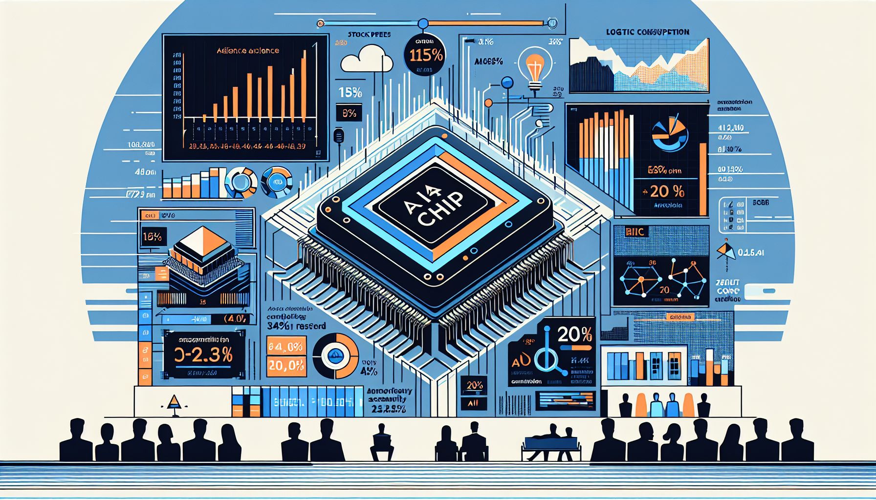
tsmc just revealed its A14 process. It promises a significant boost in AI capabilities for smartphones and other devices. The A14 is slated for production in 2028. It offers up to 15% faster speeds or 30% less power consumption compared to its predecessor. The new tech also achieves over 20% greater logic density. These advancements are critical as everyday devices adopt more AI functionality. The company’s North America Technology Symposium had over 2,500 attendees.
driving ai transformation
TSMC’s A14 process is engineered to accelerate AI transformation. It achieves this by delivering faster computing and greater power efficiency [1][7]. Smartphones are expected to benefit through enhanced on-device AI capabilities [1][5]. TSMC is also evolving its NanoFlex architecture to NanoFlex Pro [1][7]. This evolution enables superior performance, greater power efficiency, and enhanced design flexibility [1]. TSMC’s advancements are poised to significantly impact the integration of AI in various applications [1][8].
advanced packaging and high-performance computing
TSMC is also focusing on advanced packaging technologies. The company plans to bring its 9.5 reticle size CoWoS (Chip on Wafer on Substrate) to volume production in 2027 [1][2]. This technology will facilitate the integration of 12 or more HBM (high-bandwidth memory) stacks within a single package [1][2]. TSMC showcased its System-on-Wafer (TSMC-SoW™) technology in 2024 and followed it with SoW-X [1][2]. SoW-X, based on CoWoS, will create a wafer-sized system with computing power 40 times greater than current CoWoS solutions, with volume production scheduled for 2027 [1].
implications for tsmc stock
The unveiling of the A14 process and related technologies can positively influence TSMC’s stock (TSM:NYSE). TSMC’s commitment to innovation and its focus on high-growth areas like AI and automotive are likely to strengthen its market position [1][2]. TSMC is also developing the N3A process for automotive applications, which is in the final stage of AEC-Q100 Grade-1 qualification [1][2]. TSMC’s ability to consistently deliver cutting-edge technology reinforces investor confidence and positions the company favorably in the semiconductor market [4].
manufacturing capacity and geopolitical risks
TSMC’s manufacturing capacity is a crucial factor in its ability to meet the demands of its advanced processes. The majority of TSMC’s chip production occurs in Taiwan [5]. This concentration introduces geopolitical risks, given the complex relationship between Taiwan and China [GPT]. Any disruption to TSMC’s operations could have significant repercussions for the global chip supply chain [GPT]. TSMC’s expansion into regions like Arizona aims to mitigate these risks by diversifying its manufacturing footprint [5].
market leadership and competition
With the A14 process, TSMC aims to maintain its leadership in semiconductor manufacturing [4]. TSMC is also planning an intermediary A16 chip process for late 2026 [4]. TSMC is facing competition from companies like Samsung and Intel, who are also investing heavily in advanced manufacturing technologies [GPT]. TSMC’s consistent advancements and its close relationships with key customers like Apple provide a competitive edge [5]. TSMC’s ability to deliver on its technology roadmap will be crucial in maintaining its market leadership [1].
Bronnen
- pr.tsmc.com
- www.bloomberg.com
- www.tomshardware.com
- www.cultofmac.com
- www.electronicsweekly.com
- www.baha.com
- www.marketscreener.com