AI-powered inspection tool promises breakthrough in semiconductor testing
Munich, Thursday, 28 November 2024.
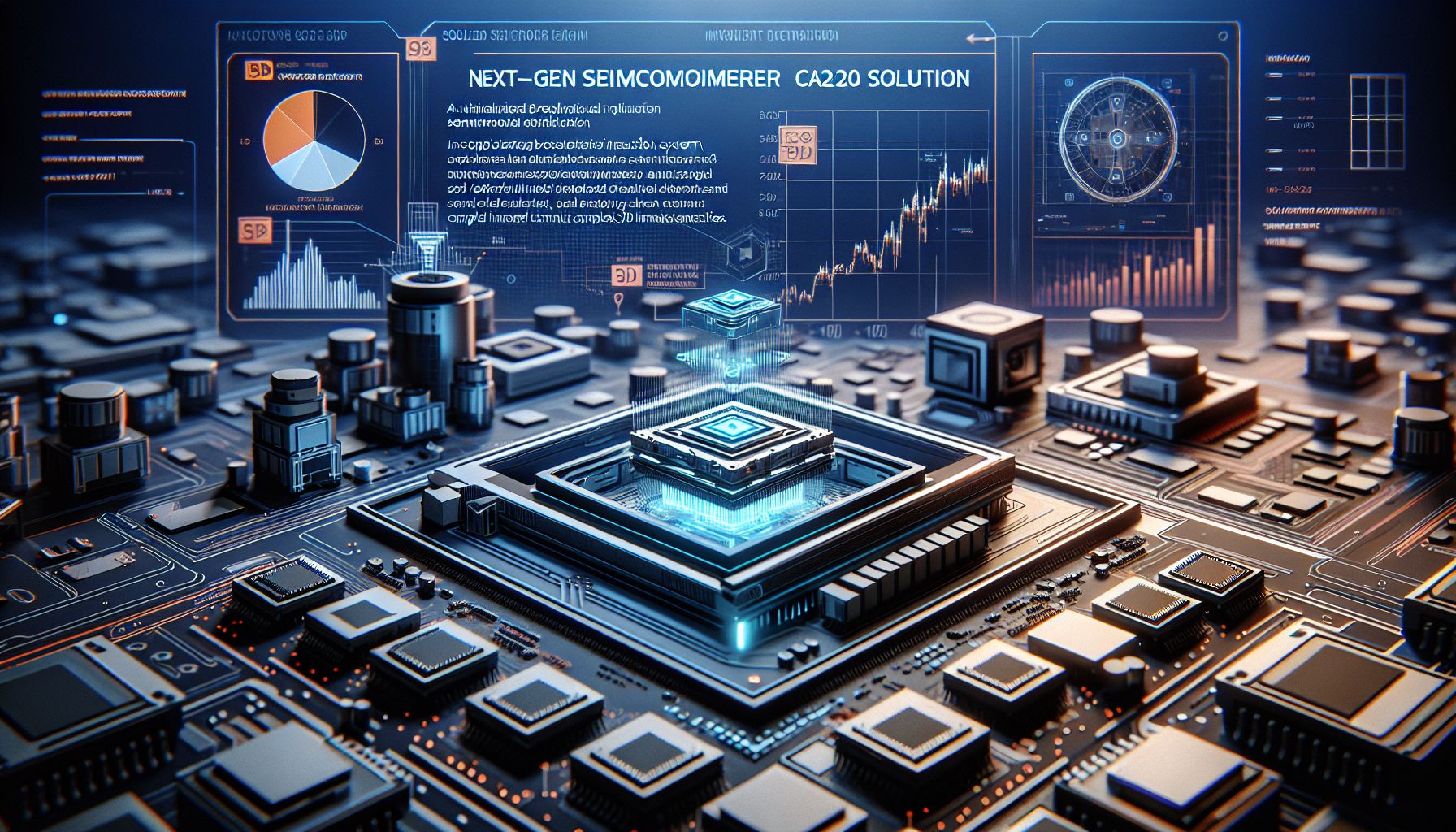
A groundbreaking automated inspection system for advanced semiconductor packaging was unveiled at Semicon Europa 2024 in Munich. The next-gen CA20 solution combines artificial intelligence with high-resolution 2D and 3D imaging capabilities to detect structural defects in complex 3D integrated circuits. This innovation arrives at a crucial time for Europe’s semiconductor industry, which is pushing to expand its global market share. The system’s AI-driven automated defect recognition specifically targets solder bump inspection, a critical component in chip manufacturing. The launch aligns with Europe’s broader strategy to address the semiconductor talent shortage and achieve sustainable growth in the sector. This development represents a significant step forward in the industry’s drive toward more efficient and precise quality control methods.
investor reactions and stock implications
The unveiling of the next-gen CA20 inspection solution at Semicon Europa 2024 has stirred significant interest among investors. The technology’s potential to revolutionize semiconductor testing could lead to increased efficiency and reduced waste. These improvements are likely to enhance profitability for companies that adopt this technology. Market analysts suggest that early adopters might see a shift in their stock value as they capitalize on the benefits of reduced defect rates and improved production yields. Comet, a key player in this innovation, may experience a positive shift in investor confidence, potentially boosting its stock performance[1].
market context and technology impact
The introduction of the CA20 inspection system comes at a pivotal moment for the semiconductor industry, particularly in Europe. With the European Chips Act aiming to strengthen local semiconductor capabilities, innovations like the CA20 are crucial. This system not only enhances manufacturing precision but also supports sustainability goals by minimizing material waste. Its AI-driven approach aligns with global trends toward automation and smart manufacturing. By integrating such advanced technologies, European companies can better compete in the global market, potentially leading to increased market share and, consequently, enhanced stock valuations[2].
expert opinions and future outlook
Industry experts at Semicon Europa highlighted the CA20’s potential to address longstanding challenges in semiconductor manufacturing. The integration of AI for defect detection represents a leap in technological capability. Experts predict that as more companies integrate this system, the semiconductor market could see a rise in overall production quality and efficiency. This could lead to a competitive advantage for European manufacturers. The focus on reducing the talent gap, as discussed during the event, further emphasizes the need for advanced tools like the CA20 to maintain industry growth. If successful, this could translate into stronger financial performance for companies involved[3].